Dr Reza Kashtiban
Restored Phase of Monolayer Garphene by Inline Holography
Curriculum VitaeLink opens in a new windowHis current research themes involves growth and compositional characterisation of encapsulated composite nanostrucures, 1D radial heterostructures and 2D materials. He has also expertise on the study of porous materials, functionalised carbon based materials and phase change nanomaterials.
Current Interests
Carbon Based Materials
2D materials
Hybrid photovoltaic nanostructures
Encapsulated structures
1D Van der Waals Heterostructures
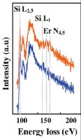
Phase Change Materials
Atomic scale local characterisation
Teaching
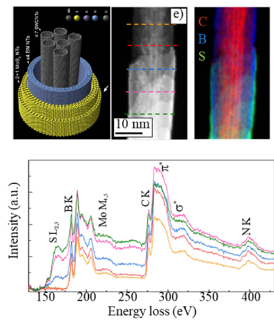
STEM-EELS of CNT/BN/MoS2 vdW Heterostructure
Selected Publications
R.J. Kashtiban, C. E. Patrick, Q. Ramasse, R. I. Walton and J. Sloan
Linear and Helical Caesium Iodide Atomic Chains in Ultra-Narrow Single Walled Carbon Nanotubes
Reza J. Kashtiban, Maria Burdanova, Andrij Vasylenko, Jamie Wynn, Paulo V. C. Meideros, Quentin Ramasse, Andrew J. Morris, David Quigley, James Lloyd-Hughes and Jeremy Sloan, , ACS Nano 15 (2021), pp 13389-13398
Maria G Burdanova, Reza J Kashtiban, Yongjia Zheng, Rong Xiang, Shohei Chiashi, Jack Matthew Woolley, Michael Staniforth, Emily Sakamoto-Rablah, Xue Xie, Matthew Broome, Jeremy Sloan, Anton Anisimov, Esko I Kauppinen, Shigeo Maruyama and James Lloyd-Hughes, Nano Lett. 20(2020) pp 3560–3567
Towards a 3D GeSbTe phase change memory with integrated selector by non-aqueous electrod
Ruomeng Huang, Gabriela P Kissling, Reza Kashtiban, Yasir J Noori, Katarina Cicvarić, Wenjian Zhang, Andrew L Hector, Richard Beanland, David C Smith, Gillian Reid, Philip N Bartlett, CH Kees de Groot, Faraday Discuss. 213 (2019) pp 339-355
R. Huag, X. Yan, S. Ye, R. J. Kashtiban, R. Beanland, K. A. Morgan, M. D. B. Charlton, C. H. de Groot,Nanoscale Research Letts. 12(2017)
Atomically Resolved Imaging of Highly Ordered Alternating Fluorinated Graphene
R. J Kashtiban, M. A. Dyson, R. R Nair, R. Zan, S. L Wong, Q. Ramasse, A. K Geim, U. Bangert, J. Sloan, Nature Comm., 5 (2014) 4902
Dr Reza Kashtiban
Associate Professor


Department of Physics
University of Warwick
Gibbet Hill Road
Coventry CV4 7AL
UK
Office: P5.68

+44 (0)2476 5 22054

r.kashtiban@warwick.ac.uk
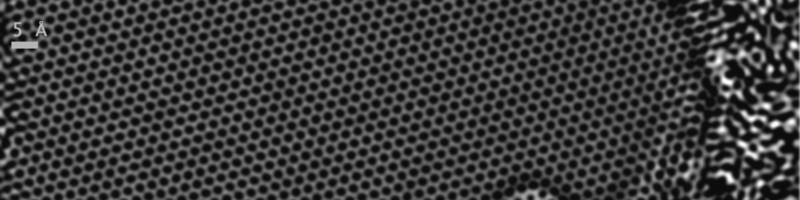
Reconstructed phase of HRTEM of Gr
phase of chair-C2F
Vice Chancellor WoW Award 2022

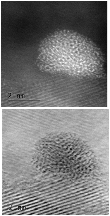
Pd catalysts particls on TiO2
STEM-ADF image of Perovskites La0.5Sm0.5CrO3
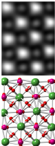
STEM-ABF image of Perovskites La0.5Sm0.5CrO3
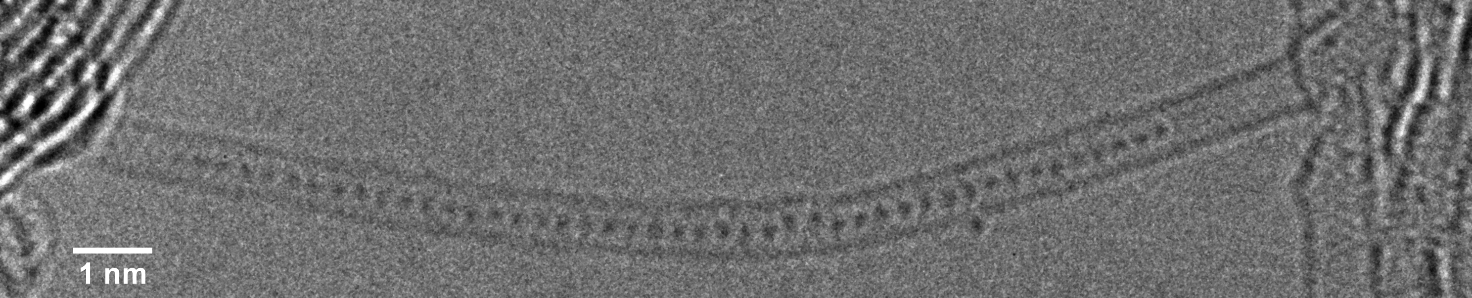
Unzipping graphene sheet under electron beam in TEM