
Quantum Devices Group
The Quantum Devices group at Warwick is interested in semiconductor devices fabricated using narrow bandgap III-V compound semiconductor materials. We are a rapidly growing group concerned with the practical challenges of fabricating devices in indium antimonide (InSb) and other closely related materials. InSb has already shown great promise for mid-wave infrared and ultra-high speed devices, with its extreme electrical properties also enabling the possibility of novel spin-based and ballistic devices. The Quantum Devices group is interested in realising the potential of InSb devices, both in the laboratory and in industrial manufacture.
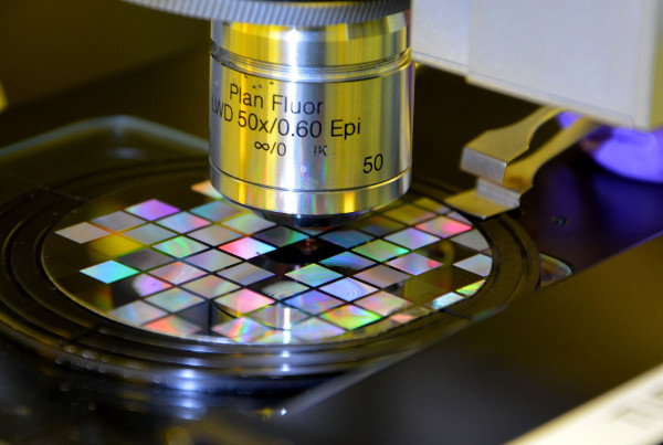
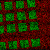
Nano-antenna test patterns under the microscope
Research
Our activities are currently focused on infrared optoelectronic devices, material interfaces and epitaxial growth techniques. We are aiming to improve infrared LEDs and photodetectors by using nano-antenna structures to improve optical coupling. By better understanding interfaces, good dielectric layers can be formed, reducing leakage currents. Our growth work aims to improve the quality of epitaxially grown layers, expand the range of materials available and improve compatability with silicon substrates.
Facilities
Our activities involve extensive use of the School of Engineering’s 'Science City' cleanroom facility, as well as epitaxial growth and device characterisation facilities in other departments at Warwick. The Science City cleanroom is a state-of-the-art process engineering facility, featuring a wide array of fabriation tools and test equipment.
Publications
A selection of publications by group members.
Head of Lab: Professor Tim Ashley
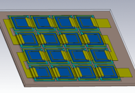
Infrared device array in simulation
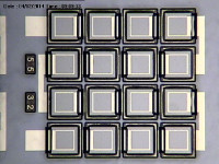
Infrared device array under optical microscope
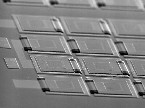
Infrared device array viewed using scanning electron microscope (SEM)
Composition imaging using X-ray photoelectron spectrometry (XPS)